


ELM631FA
28Vin up to 6A synchronous 4-switch buck-boost converter
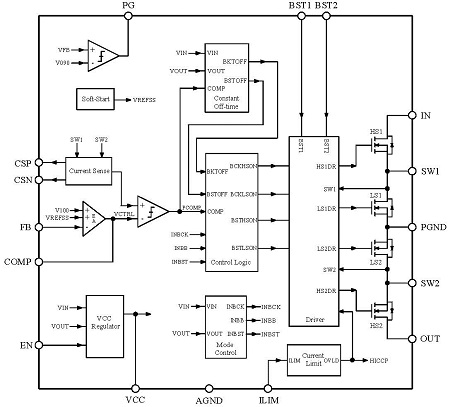
ELM631FA is a wide input range fully integrated 4-switch synchronous buck-boost converter capable of regulating the output voltage at, above, or below the input voltage. The device employs the patented peak current mode with constant off-time control scheme that significantly simplifies control loop design and offers seamless transition between Buck, Buck-Boost and Boost mode operations. Proprietary inductor DCR current sensing eliminates the need for external current sense resistor and improves system power efficiency. With external compensation, ELM631FA can be optimized to operate with a wide range of input and output voltage at all current levels. ELM631FA comes with internal soft-start, programmable inductor peak current limit, input under-voltage and over-voltage lockout, hiccup mode for short circuit or overload protection and thermal shutdown. The high integration level of ELM631FA offers great ease of use and minimizes the external components as well as board space. ELM631FA is available with a small footprint 5mmx5mm 28-lead QFN package.
| Inductor DCR current sensing | |
|---|---|
| Programmable input switch current limit | |
| Accurate EN threshold voltage | |
| Output voltage power good indicator | |
| Cycle-by-Cycle peak current limit | |
| Short circuit protection with hiccup mode | |
| Input voltage range | 3.1V to 28.0V |
| Output voltage range | 1.0V to 28.0V |
| Switch transistor | 17mΩ/20A Nch MOS×4 |
| Output current | 5A (Input voltage 4.5V to 20V) 6A (Input voltage 20V or more) |
| Efficiency | 97.5% |
| Switching frequency | 600kHz |
| Thermal shutdown | 155°C |
| Package | QFN28-5×5 Show datasheet |
| Datasheet | ELM631FA |
- Application
- USB type C hub
- 5V, 9V, 12V, 20V and 24V VDC bus power
- USB-PD and thunderbolt ports for PCs
- Power banks and electronic cigarette
- Tablet computer accessories
- Industrial battery powered systems
Absolute Maximum Ratings
| Parameter | Symbol | Limit | Unit |
|---|---|---|---|
| VIN-AGND Supply voltage | Vin | -0.3 to +30.0 | V |
| VOUT-AGND Supply voltage | Vout | -0.3 to +30.0 | V |
| EN-AGND Supply voltage | Ven | -0.3 to +30.0 | V |
| CSP-AGND Supply voltage | Vcsp | -0.3 to +30.0 | V |
| CSN-AGND Supply voltage | Vcsn | -0.3 to +30.0 | V |
| CSP-CSN Supply voltage | Vcsp-csn | -0.3 to +0.3 | V |
| SW1-AGND Supply voltage | Vsw1-agnd | -0.3 to Vin+0.6 | V |
| Dynamic SW1 in 50ns duration | Vsw1 | -3 to Vin+3 | V |
| SW2-AGND Supply voltage | Vsw2-agnd | -0.3 to Vout+0.6 | V |
| Dynamic SW2 in 50ns duration | Vsw2 | 3 to Vout+3 | V |
| BST1-SW1 Supply voltage | Vbst1-sw1 | -0.3 to +6.0 | V |
| BST2-SW2 Supply voltage | Vbst2-sw2 | -0.3 to +6.0 | V |
| PGND-AGND Supply voltage | Vpgnd-agnd | -0.3 to +0.3 | V |
| The other pins to AGND | Vother | -0.3 to +6.0 | V |
| Lead temperature | TL | +260 | °C |
| Junction temperature range | Tj | -40 to +150 | °C |
| Storage temperature range | Tstg | -55 to +150 | °C |
| Thermal resistance | θja | 35.6 | °C/W |
| Thermal resistance | θjc | 12.0 | °C/W |
| Power dissipation | Pd | 3.5 | W |
Block diagram